1N5405 datasheet
For use in general purpose rectification of power supplies, inverters, converters and freewheeling diodes application.
CHARACTERISTICS 1N5405
| Maximum repetitive peak reverse voltage | VRRM | 500 | V |
| Maximum RMS voltage | VRMS | 350 | V |
| Maximum DC blocking voltage | VDC | 500 | V |
| Maximum instantaneous forward voltage 3.0 A | VF | 1.2 | V |
| Maximum average forward rectified current 0.5″ (12.5 mm) lead length at T L = 105 °C | IF(AV) | 3.0 | А |
| Peak forward surge current 8.3 ms single half sine-wave superimposed on rated load | IFSM | 200 | А |
| Maximum DC reverse current at rated DC blocking voltage TA = 25 °C TA = 150 °C | IR | 5.0 500 | μA |
| Maximum full load reverse current, full cycle average 0.5″ (12.5 mm) lead length at TL = 105 °C | IR(AV) | 500 | μA |
| Operating junction and storage temperature range | TJ , TSTG | -50 to +150 | °C |
| Typical junction capacitance. (4.0 V, 1 MHz) | CJ | 30 | pF |
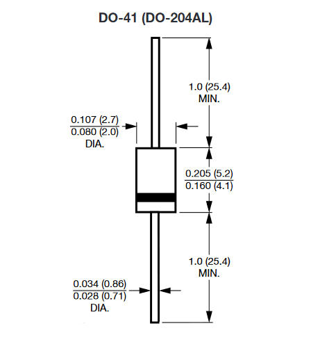
PACKAGE OUTLINE DIMENSIONS in inches (millimeters)
Case: DO-201AD, molded epoxy body
Molding compound meets UL 94 V-0 flammability rating
Base P/N-E3 – RoHS-compliant, commercial grade
Terminals: Matte tin plated leads, solderable per
J-STD-002 and JESD 22-B102
E3 suffix meets JESD 201 class 1A whisker test
Polarity: Color band denotes cathode end

